# K230 lpddr3/lpddr4 Driver Adaptation Guide
## Overview
This document mainly introduces the adaptation and testing methods for the K230 LPDDR driver, covering the configuration of key parameters such as Swap, ODT, Impedance, and Vref (reference voltage).
>When replacing the DRAM chip or when DDR-related PCB traces are changed, **parameter adaptation must be re-performed**, and after adaptation is completed, refer to [DDR Stress Test](#ddr-stress-test) to **execute the DDR stress test** to verify memory stability.
## K230 DDR Description
The k230/k230d ddr driver is under the board directory in uboot. The common board driver file descriptions are as follows:
| uboot code path | Driver description |
| -------------------------------------------------------------- | ---------------------------------------- |
| board/canaan/k230_canmv_01studio/lpddr4_init_32_swap_2667.c | 01studio board lpddr4 2667 driver |
| board/canaan/k230_canmv_01studio/lpddr4_init_32_swap_3200.c | 01studio board lpddr4 3200 driver |
| board/canaan/common/sip_lpddr4_init_32_swap_2667.c | k230d internal lpddr4 2667 driver |
| board/canaan/common/sip_lpddr4_init_32_swap_1600.c | k230d internal lpddr4 1600 driver |
| board/canaan/common/sip_lpddr4_init_32_swap_3200_with_allodt.c | k230d internal lpddr4 3200 driver (all odt enabled) |
| board/canaan/common/sip_lpddr4_init_32_swap_3200_with_wodt.c | k230d internal lpddr4 3200 driver (write odt only enabled) |
| board/canaan/k230_canmv_dongshanpi/canmv_ddr_init_2133.c | 100ask lpddr3 2133 driver |
| board/canaan/k230_canmv_dongshanpi/canmv_ddr_init_1866.c | 100ask lpddr3 1866 driver |
| board/canaan/k230_unsiplp4/lpddr4_init_32_swap_3200.c | evb lpddr4 3200 driver |
| board/canaan/k230_unsiplp4/lpddr4_init_32_swap_2667.c | evb lpddr3 2667 driver |
| board/canaan/k230_evb/ddr_init_2133.c | evb lpddr3 2133 driver |
lpddr4 recommends 2667, lpddr3 recommends 2133. Please refer to the above files (recommended reference files are shown in the table below) for ddr driver adaptation. The places that need to be modified are described later in this document.
| ddr driver recommended reference file | Description |
| -------------------------------------------------------------- | ---------------------------- |
| board/canaan/k230_canmv_01studio/lpddr4_init_32_swap_2667.c | k230 lpddr4 2667 |
| board/canaan/k230_canmv/lpddr4_init_32_swap_3200.c | k230 lpddr4 3200 |
| board/canaan/k230_canmv/k230pi_ddr_init_2133.c | k230 lpddr3 2133 |
| board/canaan/k230_canmv_dongshanpi/canmv_ddr_init_1866.c | k230 lpddr3 1866 |
| board/canaan/k230_evb/lpddr3_swap_1600.c | k230 lpddr3 1600 |
| board/canaan/common/sip_lpddr4_init_32_swap_2667.c | k230d internal lpddr4 2667 driver |
| board/canaan/common/sip_lpddr4_init_32_swap_1600.c | k230d internal lpddr4 1600 driver |
| board/canaan/common/sip_lpddr4_init_32_swap_3200_with_allodt.c | k230d internal lpddr4 3200 driver |
## LPDDR4 swap
### lpddr4 swap description
Recommendation:
Within an LPDDR4 byte group, DQ can be swapped; DQ swap between bytes is not supported; byte-to-byte swap is supported within a channel group.
It is recommended to perform routing according to the reference board. When designing on your own, if the swap is modified, the ddr driver (training) code needs to be adjusted. Refer to the following sections for modification methods.
Theoretical requirements:
1. ODT, CK, CKE, CS can't be swap.
1. DQ can be swapped with any other DQ that in the same Byte
1. For LPDDR4 the Byte swap can only occur within a channel, for LPDDR4, DBYTE0 could only be swapped with DBYTE1; DBYTE2 could only be swapped with DBYTE3, and it don’t need to modify Firmware;
1. Within an LPDDR4 byte group, DQ can be swapped; DQ swap between bytes is not supported; byte-to-byte swap is supported within a channel group.
1. DQS/DM must be swap along with the corresonding DBYTE swap. in the internal DBYTE, DQS/DM are not allowed swappend.
1. For LPDDR4, CA could be swapped within the same channel,and should modify the Firmware to accommodate this.
### Adjustment Rules
For the adjustment rules, see the figure below. The register base address on the left is adjusted according to the red part on the right, the bit position on the left is adjusted according to the yellow part on the right, and the CA bit number on the left is adjusted according to the green part on the right.
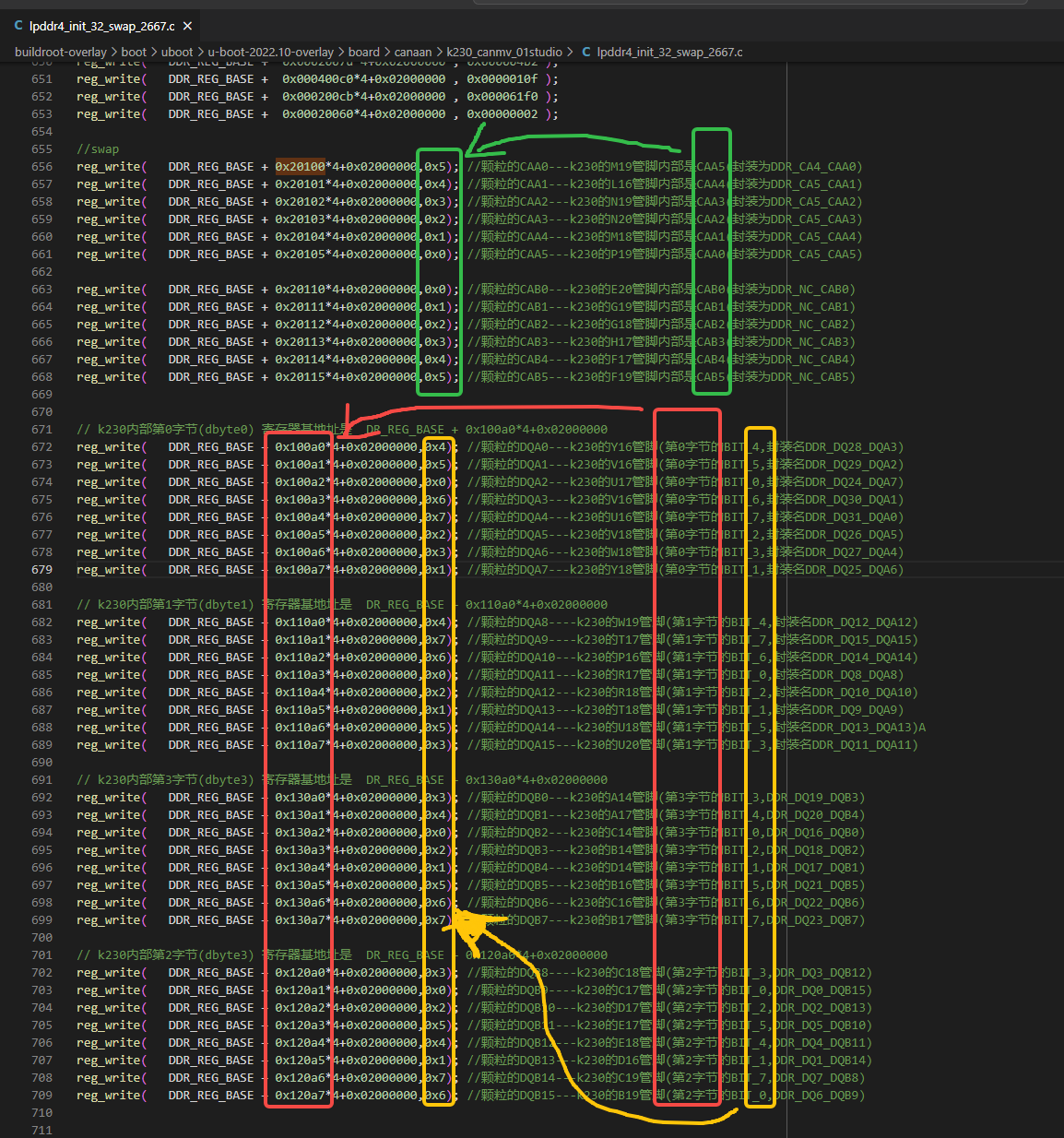
>For ddr pin and function definitions, please refer to the [K230 DDR Pin Definition Table](#k230-ddr-pin-definition-table)
### Example 1: 01studio lpddr4 Driver
Part of the 01studio lpddr4 schematic and driver code are as follows:
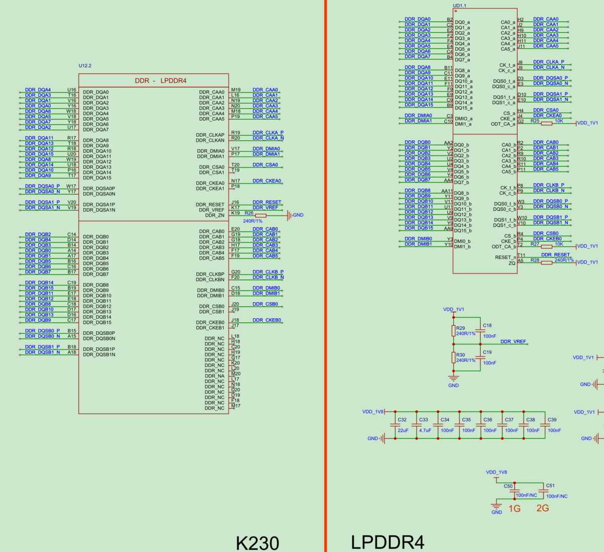
```c
//01studio board ddr driver code snippet
//https://github.com/kendryte/k230_linux_sdk/blob/dev/buildroot-overlay/boot/uboot/u-boot-2022.10-overlay/board/canaan/k230_canmv_01studio/lpddr4_init_32_swap_2667.c
//swap
reg_write( DDR_REG_BASE + 0x20100*4+0x02000000,0x5); //颗粒的CAA0---k230的M19管脚内部是CAA5(封装为DDR_CA4_CAA0)
reg_write( DDR_REG_BASE + 0x20101*4+0x02000000,0x4); //颗粒的CAA1---k230的L16管脚内部是CAA4(封装为DDR_CA5_CAA1)
reg_write( DDR_REG_BASE + 0x20102*4+0x02000000,0x3); //颗粒的CAA2---k230的N19管脚内部是CAA3(封装为DDR_CA5_CAA2)
reg_write( DDR_REG_BASE + 0x20103*4+0x02000000,0x2); //颗粒的CAA3---k230的N20管脚内部是CAA2(封装为DDR_CA5_CAA3)
reg_write( DDR_REG_BASE + 0x20104*4+0x02000000,0x1); //颗粒的CAA4---k230的M18管脚内部是CAA1(封装为DDR_CA5_CAA4)
reg_write( DDR_REG_BASE + 0x20105*4+0x02000000,0x0); //颗粒的CAA5---k230的P19管脚内部是CAA0(封装为DDR_CA5_CAA5)
reg_write( DDR_REG_BASE + 0x20110*4+0x02000000,0x0); //颗粒的CAB0---k230的E20管脚内部是CAB0(封装为DDR_NC_CAB0)
reg_write( DDR_REG_BASE + 0x20111*4+0x02000000,0x1); //颗粒的CAB1---k230的G19管脚内部是CAB1(封装为DDR_NC_CAB1)
reg_write( DDR_REG_BASE + 0x20112*4+0x02000000,0x2); //颗粒的CAB2---k230的G18管脚内部是CAB2(封装为DDR_NC_CAB2)
reg_write( DDR_REG_BASE + 0x20113*4+0x02000000,0x3); //颗粒的CAB3---k230的H17管脚内部是CAB3(封装为DDR_NC_CAB3)
reg_write( DDR_REG_BASE + 0x20114*4+0x02000000,0x4); //颗粒的CAB4---k230的F17管脚内部是CAB4(封装为DDR_NC_CAB4)
reg_write( DDR_REG_BASE + 0x20115*4+0x02000000,0x5); //颗粒的CAB5---k230的F19管脚内部是CAB5(封装为DDR_NC_CAB5)
// k230内部第0字节(dbyte0) 寄存器基地址是 DR_REG_BASE + 0x100a0*4+0x02000000
reg_write( DDR_REG_BASE + 0x100a0*4+0x02000000,0x4); //颗粒的DQA0---k230的Y16管脚(第0字节的BIT_4,封装名DDR_DQ28_DQA3)
reg_write( DDR_REG_BASE + 0x100a1*4+0x02000000,0x5); //颗粒的DQA1---k230的V16管脚(第0字节的BIT_5,封装名DDR_DQ29_DQA2)
reg_write( DDR_REG_BASE + 0x100a2*4+0x02000000,0x0); //颗粒的DQA2---k230的U17管脚(第0字节的BIT_0,封装名DDR_DQ24_DQA7)
reg_write( DDR_REG_BASE + 0x100a3*4+0x02000000,0x6); //颗粒的DQA3---k230的V16管脚(第0字节的BIT_6,封装名DDR_DQ30_DQA1)
reg_write( DDR_REG_BASE + 0x100a4*4+0x02000000,0x7); //颗粒的DQA4---k230的U16管脚(第0字节的BIT_7,封装名DDR_DQ31_DQA0)
reg_write( DDR_REG_BASE + 0x100a5*4+0x02000000,0x2); //颗粒的DQA5---k230的V18管脚(第0字节的BIT_2,封装名DDR_DQ26_DQA5)
reg_write( DDR_REG_BASE + 0x100a6*4+0x02000000,0x3); //颗粒的DQA6---k230的W18管脚(第0字节的BIT_3,封装名DDR_DQ27_DQA4)
reg_write( DDR_REG_BASE + 0x100a7*4+0x02000000,0x1); //颗粒的DQA7---k230的Y18管脚(第0字节的BIT_1,封装名DDR_DQ25_DQA6)
// k230内部第1字节(dbyte1) 寄存器基地址是 DR_REG_BASE + 0x110a0*4+0x02000000
reg_write( DDR_REG_BASE + 0x110a0*4+0x02000000,0x4); //颗粒的DQA8----k230的W19管脚(第1字节的BIT_4,封装名DDR_DQ12_DQA12)
reg_write( DDR_REG_BASE + 0x110a1*4+0x02000000,0x7); //颗粒的DQA9----k230的T17管脚(第1字节的BIT_7,封装名DDR_DQ15_DQA15)
reg_write( DDR_REG_BASE + 0x110a2*4+0x02000000,0x6); //颗粒的DQA10---k230的P16管脚(第1字节的BIT_6,封装名DDR_DQ14_DQA14)
reg_write( DDR_REG_BASE + 0x110a3*4+0x02000000,0x0); //颗粒的DQA11---k230的R17管脚(第1字节的BIT_0,封装名DDR_DQ8_DQA8)
reg_write( DDR_REG_BASE + 0x110a4*4+0x02000000,0x2); //颗粒的DQA12---k230的R18管脚(第1字节的BIT_2,封装名DDR_DQ10_DQA10)
reg_write( DDR_REG_BASE + 0x110a5*4+0x02000000,0x1); //颗粒的DQA13---k230的T18管脚(第1字节的BIT_1,封装名DDR_DQ9_DQA9)
reg_write( DDR_REG_BASE + 0x110a6*4+0x02000000,0x5); //颗粒的DQA14---k230的U18管脚(第1字节的BIT_5,封装名DDR_DQ13_DQA13)A
reg_write( DDR_REG_BASE + 0x110a7*4+0x02000000,0x3); //颗粒的DQA15---k230的U20管脚(第1字节的BIT_3,封装名DDR_DQ11_DQA11)
// k230内部第3字节(dbyte3) 寄存器基地址是 DR_REG_BASE + 0x130a0*4+0x02000000
reg_write( DDR_REG_BASE + 0x130a0*4+0x02000000,0x3); //颗粒的DQB0---k230的A14管脚(第3字节的BIT_3,DDR_DQ19_DQB3)
reg_write( DDR_REG_BASE + 0x130a1*4+0x02000000,0x4); //颗粒的DQB1---k230的A17管脚(第3字节的BIT_4,DDR_DQ20_DQB4)
reg_write( DDR_REG_BASE + 0x130a2*4+0x02000000,0x0); //颗粒的DQB2---k230的C14管脚(第3字节的BIT_0,DDR_DQ16_DQB0)
reg_write( DDR_REG_BASE + 0x130a3*4+0x02000000,0x2); //颗粒的DQB3---k230的B14管脚(第3字节的BIT_2,DDR_DQ18_DQB2)
reg_write( DDR_REG_BASE + 0x130a4*4+0x02000000,0x1); //颗粒的DQB4---k230的D14管脚(第3字节的BIT_1,DDR_DQ17_DQB1)
reg_write( DDR_REG_BASE + 0x130a5*4+0x02000000,0x5); //颗粒的DQB5---k230的B16管脚(第3字节的BIT_5,DDR_DQ21_DQB5)
reg_write( DDR_REG_BASE + 0x130a6*4+0x02000000,0x6); //颗粒的DQB6---k230的C16管脚(第3字节的BIT_6,DDR_DQ22_DQB6)
reg_write( DDR_REG_BASE + 0x130a7*4+0x02000000,0x7); //颗粒的DQB7---k230的B17管脚(第3字节的BIT_7,DDR_DQ23_DQB7)
// k230内部第2字节(dbyte3) 寄存器基地址是 DR_REG_BASE + 0x120a0*4+0x02000000
reg_write( DDR_REG_BASE + 0x120a0*4+0x02000000,0x3); //颗粒的DQB8----k230的C18管脚(第2字节的BIT_3,DDR_DQ3_DQB12)
reg_write( DDR_REG_BASE + 0x120a1*4+0x02000000,0x0); //颗粒的DQB9----k230的C17管脚(第2字节的BIT_0,DDR_DQ0_DQB15)
reg_write( DDR_REG_BASE + 0x120a2*4+0x02000000,0x2); //颗粒的DQB10---k230的D17管脚(第2字节的BIT_2,DDR_DQ2_DQB13)
reg_write( DDR_REG_BASE + 0x120a3*4+0x02000000,0x5); //颗粒的DQB11---k230的E17管脚(第2字节的BIT_5,DDR_DQ5_DQB10)
reg_write( DDR_REG_BASE + 0x120a4*4+0x02000000,0x4); //颗粒的DQB12---k230的E18管脚(第2字节的BIT_4,DDR_DQ4_DQB11)
reg_write( DDR_REG_BASE + 0x120a5*4+0x02000000,0x1); //颗粒的DQB13---k230的D16管脚(第2字节的BIT_1,DDR_DQ1_DQB14)
reg_write( DDR_REG_BASE + 0x120a6*4+0x02000000,0x7); //颗粒的DQB14---k230的C19管脚(第2字节的BIT_7,DDR_DQ7_DQB8)
reg_write( DDR_REG_BASE + 0x120a7*4+0x02000000,0x6); //颗粒的DQB15---k230的B19管脚(第2字节的BIT_6,DDR_DQ6_DQB9)
```
### Example 2: evb unsip lpddr4 Driver
Schematic:
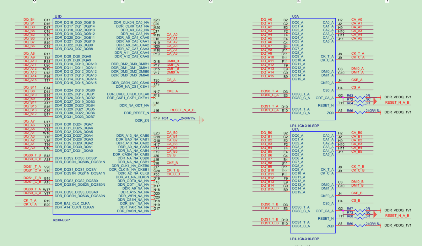
Code:
```c
//buildroot-overlay/boot/uboot/u-boot-2022.10-overlay/board/canaan/k230_unsiplp4/lpddr4_init_32_swap_3200.c
//swap
reg_write( DDR_REG_BASE + 0x20100*4+0x02000000,0x5); //颗粒的CAA0---k230的M19管脚内部是CAA5(封装为DDR_CA4_CAA0)
reg_write( DDR_REG_BASE + 0x20101*4+0x02000000,0x4); //颗粒的CAA1---k230的L16管脚内部是CAA4(封装为DDR_CA5_CAA1)
reg_write( DDR_REG_BASE + 0x20102*4+0x02000000,0x3); //颗粒的CAA2---k230的N19管脚内部是CAA3(封装为DDR_CA5_CAA2)
reg_write( DDR_REG_BASE + 0x20103*4+0x02000000,0x2); //颗粒的CAA3---k230的N20管脚内部是CAA2(封装为DDR_CA5_CAA3)
reg_write( DDR_REG_BASE + 0x20104*4+0x02000000,0x1); //颗粒的CAA4---k230的M18管脚内部是CAA1(封装为DDR_CA5_CAA4)
reg_write( DDR_REG_BASE + 0x20105*4+0x02000000,0x0); //颗粒的CAA5---k230的P19管脚内部是CAA0(封装为DDR_CA5_CAA5)
reg_write( DDR_REG_BASE + 0x20110*4+0x02000000,0x0); //颗粒的CAB0---k230的E20管脚内部是CAB0(封装为DDR_NC_CAB0)
reg_write( DDR_REG_BASE + 0x20111*4+0x02000000,0x1); //颗粒的CAB1---k230的G19管脚内部是CAB1(封装为DDR_NC_CAB1)
reg_write( DDR_REG_BASE + 0x20112*4+0x02000000,0x2); //颗粒的CAB2---k230的G18管脚内部是CAB2(封装为DDR_NC_CAB2)
reg_write( DDR_REG_BASE + 0x20113*4+0x02000000,0x3); //颗粒的CAB3---k230的H17管脚内部是CAB3(封装为DDR_NC_CAB3)
reg_write( DDR_REG_BASE + 0x20114*4+0x02000000,0x4); //颗粒的CAB4---k230的F17管脚内部是CAB4(封装为DDR_NC_CAB4)
reg_write( DDR_REG_BASE + 0x20115*4+0x02000000,0x5); //颗粒的CAB5---k230的F19管脚内部是CAB5(封装为DDR_NC_CAB5)
// k230内部第0字节(dbyte0) 寄存器基地址是 DR_REG_BASE + 0x100a0*4+0x02000000
reg_write( DDR_REG_BASE + 0x100a0*4+0x02000000,0x7); //颗粒的DQA0---k230的U16管脚(第0字节的BIT_7,封装名DDR_DQ31_DQA0)
reg_write( DDR_REG_BASE + 0x100a1*4+0x02000000,0x6); //颗粒的DQA1---k230的V16管脚(第0字节的BIT_6,封装名DDR_DQ30_DQA1)
reg_write( DDR_REG_BASE + 0x100a2*4+0x02000000,0x5); //颗粒的DQA2---k230的V16管脚(第0字节的BIT_5,封装名DDR_DQ29_DQA2)
reg_write( DDR_REG_BASE + 0x100a3*4+0x02000000,0x4); //颗粒的DQA3---k230的Y16管脚(第0字节的BIT_4,封装名DDR_DQ28_DQA3)
reg_write( DDR_REG_BASE + 0x100a4*4+0x02000000,0x3); //颗粒的DQA4---k230的W18管脚(第0字节的BIT_3,封装名DDR_DQ27_DQA4)
reg_write( DDR_REG_BASE + 0x100a5*4+0x02000000,0x2); //颗粒的DQA5---k230的V18管脚(第0字节的BIT_2,封装名DDR_DQ26_DQA5)
reg_write( DDR_REG_BASE + 0x100a6*4+0x02000000,0x1); //颗粒的DQA6---k230的Y18管脚(第0字节的BIT_1,封装名DDR_DQ25_DQA6)
reg_write( DDR_REG_BASE + 0x100a7*4+0x02000000,0x0); //颗粒的DQA7---k230的U17管脚(第0字节的BIT_0,封装名DDR_DQ24_DQA7)
// k230内部第1字节(dbyte1) 寄存器基地址是 DR_REG_BASE + 0x110a0*4+0x02000000
reg_write( DDR_REG_BASE + 0x110a0*4+0x02000000,0x0); //颗粒的DQA8----k230的R17管脚(第1字节的BIT_0,封装名DDR_DQ8_DQA8)
reg_write( DDR_REG_BASE + 0x110a1*4+0x02000000,0x1); //颗粒的DQA9----k230的T18管脚(第1字节的BIT_1,封装名DDR_DQ9_DQA9)
reg_write( DDR_REG_BASE + 0x110a2*4+0x02000000,0x2); //颗粒的DQA10---k230的R18管脚(第1字节的BIT_2,封装名DDR_DQ10_DQA10)
reg_write( DDR_REG_BASE + 0x110a3*4+0x02000000,0x3); //颗粒的DQA11---k230的U20管脚(第1字节的BIT_3,封装名DDR_DQ11_DQA11)
reg_write( DDR_REG_BASE + 0x110a4*4+0x02000000,0x4); //颗粒的DQA12---k230的W19管脚(第1字节的BIT_4,封装名DDR_DQ12_DQA12)
reg_write( DDR_REG_BASE + 0x110a5*4+0x02000000,0x5); //颗粒的DQA13---k230的U18管脚(第1字节的BIT_5,封装名DDR_DQ13_DQA13)
reg_write( DDR_REG_BASE + 0x110a6*4+0x02000000,0x6); //颗粒的DQA14---k230的P16管脚(第1字节的BIT_6,封装名DDR_DQ14_DQA14)
reg_write( DDR_REG_BASE + 0x110a7*4+0x02000000,0x7); //颗粒的DQA15---k230的T17管脚(第1字节的BIT_7,封装名DDR_DQ15_DQA15)
//// k230内部第3字节(dbyte3) 寄存器基地址是 DR_REG_BASE + 0x130a0*4+0x02000000
reg_write( DDR_REG_BASE + 0x130a0*4+0x02000000,0x1); //颗粒的DQB0---k230的D14管脚(第3字节的BIT_1,DDR_DQ17_DQB1)
reg_write( DDR_REG_BASE + 0x130a1*4+0x02000000,0x3); //颗粒的DQB1---k230的A14管脚(第3字节的BIT_3,DDR_DQ19_DQB3)
reg_write( DDR_REG_BASE + 0x130a2*4+0x02000000,0x2); //颗粒的DQB2---k230的B14管脚(第3字节的BIT_2,DDR_DQ18_DQB2)
reg_write( DDR_REG_BASE + 0x130a3*4+0x02000000,0x0); //颗粒的DQB3---k230的C14管脚(第3字节的BIT_0,DDR_DQ16_DQB0)
reg_write( DDR_REG_BASE + 0x130a4*4+0x02000000,0x7); //颗粒的DQB4---k230的B17管脚(第3字节的BIT_7,DDR_DQ23_DQB7)
reg_write( DDR_REG_BASE + 0x130a5*4+0x02000000,0x6); //颗粒的DQB5---k230的C16管脚(第3字节的BIT_6,DDR_DQ22_DQB6)
reg_write( DDR_REG_BASE + 0x130a6*4+0x02000000,0x4); //颗粒的DQB6---k230的A17管脚(第3字节的BIT_4,DDR_DQ20_DQB4)
reg_write( DDR_REG_BASE + 0x130a7*4+0x02000000,0x5); //颗粒的DQB7---k230的B16管脚(第3字节的BIT_5,DDR_DQ21_DQB5)
// k230内部第2字节(dbyte3) 寄存器基地址是 DR_REG_BASE + 0x120a0*4+0x02000000
reg_write( DDR_REG_BASE + 0x120a0*4+0x02000000,0x2); //颗粒的DQB8----k230的D17管脚(第2字节的BIT_2,DDR_DQ2_DQB13)
reg_write( DDR_REG_BASE + 0x120a1*4+0x02000000,0x1); //颗粒的DQB9----k230的D16管脚(第2字节的BIT_1,DDR_DQ1_DQB14)
reg_write( DDR_REG_BASE + 0x120a2*4+0x02000000,0x4); //颗粒的DQB10---k230的E18管脚(第2字节的BIT_4,DDR_DQ4_DQB11)
reg_write( DDR_REG_BASE + 0x120a3*4+0x02000000,0x5); //颗粒的DQB11---k230的E17管脚(第2字节的BIT_5,DDR_DQ5_DQB10)
reg_write( DDR_REG_BASE + 0x120a4*4+0x02000000,0x0); //颗粒的DQB12---k230的C17管脚(第2字节的BIT_0,DDR_DQ0_DQB15)
reg_write( DDR_REG_BASE + 0x120a5*4+0x02000000,0x3); //颗粒的DQB13---k230的C18管脚(第2字节的BIT_3,DDR_DQ3_DQB12)
reg_write( DDR_REG_BASE + 0x120a6*4+0x02000000,0x7); //颗粒的DQB14---k230的C19管脚(第2字节的BIT_7,DDR_DQ7_DQB8)
reg_write( DDR_REG_BASE + 0x120a7*4+0x02000000,0x6); //颗粒的DQB15---k230的B19管脚(第2字节的BIT_6,DDR_DQ6_DQB9)
```
## LPDDR3 DQ swap
### Description
Recommendation:
Within an LPDDR3 byte group, DQ can be swapped; DQ swap between bytes is not supported, and swap between bytes and bytes is not supported.
Theoretical Requirements:
1. ODT, CK, CKE, CS can't be swap.
1. DQ can be swapped with any other DQ that in the same Byte
1. For LPDDR3, the four Dbytes could be swapped arbitrarily, and should modify the Firmware to accommodate this.
1. DQS/DM must be swap along with the corresonding DBYTE swap. in the internal DBYTE, DQS/DM are not allowed swappend.
1. For LPDDR3 CA pins could be swapped arbitrary.,and should modify the Firmware to accommodate this.
### Adjustment Rules
Adjustment rules are shown in the figure below. The left register base address is adjusted according to the red part on the right, the left bit position is adjusted according to the yellow part on the right, and the left ca position number is adjusted according to the green part on the right.
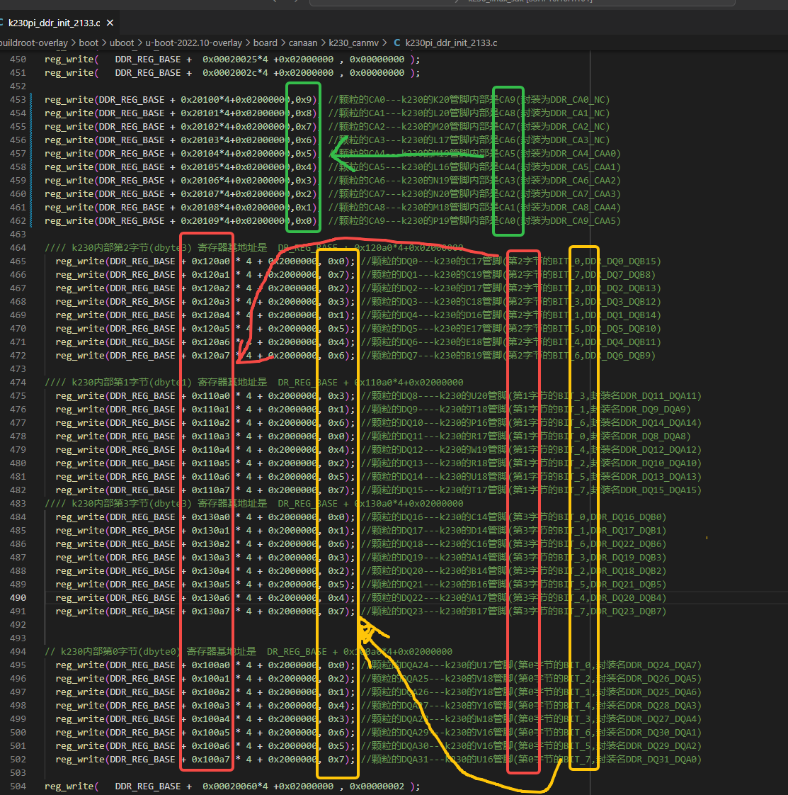
>ddr pin and function definition can refer to the [ddr related pin definition table](#k230-ddr-pin-definition-table)
### Example 1: canmv v1.1 lpddr3
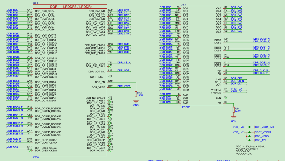
```c
//buildroot-overlay/boot/uboot/u-boot-2022.10-overlay/board/canaan/k230_canmv/k230pi_ddr_init_2133.c
reg_write(DDR_REG_BASE + 0x20100*4+0x02000000,0x9); //颗粒的CA0---k230的K20管脚内部是CA9(封装为DDR_CA0_NC)
reg_write(DDR_REG_BASE + 0x20101*4+0x02000000,0x8); //颗粒的CA1---k230的L20管脚内部是CA8(封装为DDR_CA1_NC)
reg_write(DDR_REG_BASE + 0x20102*4+0x02000000,0x7); //颗粒的CA2---k230的M20管脚内部是CA7(封装为DDR_CA2_NC)
reg_write(DDR_REG_BASE + 0x20103*4+0x02000000,0x6); //颗粒的CA3---k230的L17管脚内部是CA6(封装为DDR_CA3_NC)
reg_write(DDR_REG_BASE + 0x20104*4+0x02000000,0x5); //颗粒的CA4---k230的M19管脚内部是CA5(封装为DDR_CA4_CAA0)
reg_write(DDR_REG_BASE + 0x20105*4+0x02000000,0x4); //颗粒的CA5---k230的L16管脚内部是CA4(封装为DDR_CA5_CAA1)
reg_write(DDR_REG_BASE + 0x20106*4+0x02000000,0x3); //颗粒的CA6---k230的N19管脚内部是CA3(封装为DDR_CA6_CAA2)
reg_write(DDR_REG_BASE + 0x20107*4+0x02000000,0x2); //颗粒的CA7---k230的N20管脚内部是CA2(封装为DDR_CA7_CAA3)
reg_write(DDR_REG_BASE + 0x20108*4+0x02000000,0x1); //颗粒的CA8---k230的M18管脚内部是CA1(封装为DDR_CA8_CAA4)
reg_write(DDR_REG_BASE + 0x20109*4+0x02000000,0x0); //颗粒的CA9---k230的P19管脚内部是CA0(封装为DDR_CA9_CAA5)
//// k230内部第2字节(dbyte3) 寄存器基地址是 DR_REG_BASE + 0x120a0*4+0x02000000
reg_write(DDR_REG_BASE + 0x120a0 * 4 + 0x2000000, 0x0); //颗粒的DQ0---k230的C17管脚(第2字节的BIT_0,DDR_DQ0_DQB15)
reg_write(DDR_REG_BASE + 0x120a1 * 4 + 0x2000000, 0x7); //颗粒的DQ1---k230的C19管脚(第2字节的BIT_7,DDR_DQ7_DQB8)
reg_write(DDR_REG_BASE + 0x120a2 * 4 + 0x2000000, 0x2); //颗粒的DQ2---k230的D17管脚(第2字节的BIT_2,DDR_DQ2_DQB13)
reg_write(DDR_REG_BASE + 0x120a3 * 4 + 0x2000000, 0x3); //颗粒的DQ3---k230的C18管脚(第2字节的BIT_3,DDR_DQ3_DQB12)
reg_write(DDR_REG_BASE + 0x120a4 * 4 + 0x2000000, 0x1); //颗粒的DQ4---k230的D16管脚(第2字节的BIT_1,DDR_DQ1_DQB14)
reg_write(DDR_REG_BASE + 0x120a5 * 4 + 0x2000000, 0x5); //颗粒的DQ5---k230的E17管脚(第2字节的BIT_5,DDR_DQ5_DQB10)
reg_write(DDR_REG_BASE + 0x120a6 * 4 + 0x2000000, 0x4); //颗粒的DQ6---k230的E18管脚(第2字节的BIT_4,DDR_DQ4_DQB11)
reg_write(DDR_REG_BASE + 0x120a7 * 4 + 0x2000000, 0x6); //颗粒的DQ7---k230的B19管脚(第2字节的BIT_6,DDR_DQ6_DQB9)
//// k230内部第1字节(dbyte1) 寄存器基地址是 DR_REG_BASE + 0x110a0*4+0x02000000
reg_write(DDR_REG_BASE + 0x110a0 * 4 + 0x2000000, 0x3); //颗粒的DQ8----k230的U20管脚(第1字节的BIT_3,封装名DDR_DQ11_DQA11)
reg_write(DDR_REG_BASE + 0x110a1 * 4 + 0x2000000, 0x1); //颗粒的DQ9----k230的T18管脚(第1字节的BIT_1,封装名DDR_DQ9_DQA9)
reg_write(DDR_REG_BASE + 0x110a2 * 4 + 0x2000000, 0x6); //颗粒的DQ10---k230的P16管脚(第1字节的BIT_6,封装名DDR_DQ14_DQA14)
reg_write(DDR_REG_BASE + 0x110a3 * 4 + 0x2000000, 0x0); //颗粒的DQ11---k230的R17管脚(第1字节的BIT_0,封装名DDR_DQ8_DQA8)
reg_write(DDR_REG_BASE + 0x110a4 * 4 + 0x2000000, 0x4); //颗粒的DQ12---k230的W19管脚(第1字节的BIT_4,封装名DDR_DQ12_DQA12)
reg_write(DDR_REG_BASE + 0x110a5 * 4 + 0x2000000, 0x2); //颗粒的DQ13---k230的R18管脚(第1字节的BIT_2,封装名DDR_DQ10_DQA10)
reg_write(DDR_REG_BASE + 0x110a6 * 4 + 0x2000000, 0x5); //颗粒的DQ14---k230的U18管脚(第1字节的BIT_5,封装名DDR_DQ13_DQA13)
reg_write(DDR_REG_BASE + 0x110a7 * 4 + 0x2000000, 0x7); //颗粒的DQ15---k230的T17管脚(第1字节的BIT_7,封装名DDR_DQ15_DQA15)
//// k230内部第3字节(dbyte3) 寄存器基地址是 DR_REG_BASE + 0x130a0*4+0x02000000
reg_write(DDR_REG_BASE + 0x130a0 * 4 + 0x2000000, 0x0); //颗粒的DQ16---k230的C14管脚(第3字节的BIT_0,DDR_DQ16_DQB0)
reg_write(DDR_REG_BASE + 0x130a1 * 4 + 0x2000000, 0x1); //颗粒的DQ17---k230的D14管脚(第3字节的BIT_1,DDR_DQ17_DQB1)
reg_write(DDR_REG_BASE + 0x130a2 * 4 + 0x2000000, 0x6); //颗粒的DQ18---k230的C16管脚(第3字节的BIT_6,DDR_DQ22_DQB6)
reg_write(DDR_REG_BASE + 0x130a3 * 4 + 0x2000000, 0x3); //颗粒的DQ19---k230的A14管脚(第3字节的BIT_3,DDR_DQ19_DQB3)
reg_write(DDR_REG_BASE + 0x130a4 * 4 + 0x2000000, 0x2); //颗粒的DQ20---k230的B14管脚(第3字节的BIT_2,DDR_DQ18_DQB2)
reg_write(DDR_REG_BASE + 0x130a5 * 4 + 0x2000000, 0x5); //颗粒的DQ21---k230的B16管脚(第3字节的BIT_5,DDR_DQ21_DQB5)
reg_write(DDR_REG_BASE + 0x130a6 * 4 + 0x2000000, 0x4); //颗粒的DQ22---k230的A17管脚(第3字节的BIT_4,DDR_DQ20_DQB4)
reg_write(DDR_REG_BASE + 0x130a7 * 4 + 0x2000000, 0x7); //颗粒的DQ23---k230的B17管脚(第3字节的BIT_7,DDR_DQ23_DQB7)
// k230内部第0字节(dbyte0) 寄存器基地址是 DR_REG_BASE + 0x100a0*4+0x02000000
reg_write(DDR_REG_BASE + 0x100a0 * 4 + 0x2000000, 0x0); //颗粒的DQA24---k230的U17管脚(第0字节的BIT_0,封装名DDR_DQ24_DQA7)
reg_write(DDR_REG_BASE + 0x100a1 * 4 + 0x2000000, 0x2); //颗粒的DQA25---k230的V18管脚(第0字节的BIT_2,封装名DDR_DQ26_DQA5)
reg_write(DDR_REG_BASE + 0x100a2 * 4 + 0x2000000, 0x1); //颗粒的DQA26---k230的Y18管脚(第0字节的BIT_1,封装名DDR_DQ25_DQA6)
reg_write(DDR_REG_BASE + 0x100a3 * 4 + 0x2000000, 0x4); //颗粒的DQA27---k230的Y16管脚(第0字节的BIT_4,封装名DDR_DQ28_DQA3)
reg_write(DDR_REG_BASE + 0x100a4 * 4 + 0x2000000, 0x3); //颗粒的DQA28---k230的W18管脚(第0字节的BIT_3,封装名DDR_DQ27_DQA4)
reg_write(DDR_REG_BASE + 0x100a5 * 4 + 0x2000000, 0x6); //颗粒的DQA29---k230的V16管脚(第0字节的BIT_6,封装名DDR_DQ30_DQA1)
reg_write(DDR_REG_BASE + 0x100a6 * 4 + 0x2000000, 0x5); //颗粒的DQA30---k230的V16管脚(第0字节的BIT_5,封装名DDR_DQ29_DQA2)
reg_write(DDR_REG_BASE + 0x100a7 * 4 + 0x2000000, 0x7); //颗粒的DQA31---k230的U16管脚(第0字节的BIT_7,封装名DDR_DQ31_DQA0)
```
### Example 2: evb lpddr3
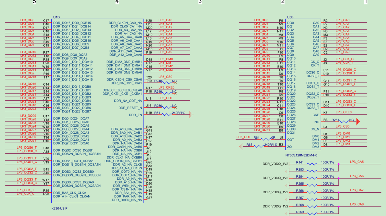
```c
//buildroot-overlay/boot/uboot/u-boot-2022.10-overlay/board/canaan/k230_evb/ddr_init_2133.c
reg_write(DDR_REG_BASE + 0x20100*4+0x02000000,0x9); //CA0
reg_write(DDR_REG_BASE + 0x20101*4+0x02000000,0x8); //CA1
reg_write(DDR_REG_BASE + 0x20102*4+0x02000000,0x7); //CA2
reg_write(DDR_REG_BASE + 0x20103*4+0x02000000,0x6); //CA3
reg_write(DDR_REG_BASE + 0x20104*4+0x02000000,0x5); //CA4
reg_write(DDR_REG_BASE + 0x20105*4+0x02000000,0x4); //CA5
reg_write(DDR_REG_BASE + 0x20106*4+0x02000000,0x3); //CA6
reg_write(DDR_REG_BASE + 0x20107*4+0x02000000,0x2); //CA7
reg_write(DDR_REG_BASE + 0x20108*4+0x02000000,0x1); //CA8
reg_write(DDR_REG_BASE + 0x20109*4+0x02000000,0x0); //CA9
reg_write(DDR_REG_BASE + 0x120a0 * 4 + 0x2000000, 0x0);
reg_write(DDR_REG_BASE + 0x120a1 * 4 + 0x2000000, 0x1);
reg_write(DDR_REG_BASE + 0x120a2 * 4 + 0x2000000, 0x2);
reg_write(DDR_REG_BASE + 0x120a3 * 4 + 0x2000000, 0x3);
reg_write(DDR_REG_BASE + 0x120a4 * 4 + 0x2000000, 0x4);
reg_write(DDR_REG_BASE + 0x120a5 * 4 + 0x2000000, 0x5);
reg_write(DDR_REG_BASE + 0x120a6 * 4 + 0x2000000, 0x6);
reg_write(DDR_REG_BASE + 0x120a7 * 4 + 0x2000000, 0x7);
reg_write(DDR_REG_BASE + 0x110a0 * 4 + 0x2000000, 0x2);
reg_write(DDR_REG_BASE + 0x110a1 * 4 + 0x2000000, 0x6);
reg_write(DDR_REG_BASE + 0x110a2 * 4 + 0x2000000, 0x0);
reg_write(DDR_REG_BASE + 0x110a3 * 4 + 0x2000000, 0x4);
reg_write(DDR_REG_BASE + 0x110a4 * 4 + 0x2000000, 0x1);
reg_write(DDR_REG_BASE + 0x110a5 * 4 + 0x2000000, 0x3);
reg_write(DDR_REG_BASE + 0x110a6 * 4 + 0x2000000, 0x5);
reg_write(DDR_REG_BASE + 0x110a7 * 4 + 0x2000000, 0x7);
reg_write(DDR_REG_BASE + 0x130a0 * 4 + 0x2000000, 0x0);
reg_write(DDR_REG_BASE + 0x130a1 * 4 + 0x2000000, 0x2);
reg_write(DDR_REG_BASE + 0x130a2 * 4 + 0x2000000, 0x6);
reg_write(DDR_REG_BASE + 0x130a3 * 4 + 0x2000000, 0x4);
reg_write(DDR_REG_BASE + 0x130a4 * 4 + 0x2000000, 0x1);
reg_write(DDR_REG_BASE + 0x130a5 * 4 + 0x2000000, 0x3);
reg_write(DDR_REG_BASE + 0x130a6 * 4 + 0x2000000, 0x7);
reg_write(DDR_REG_BASE + 0x130a7 * 4 + 0x2000000, 0x5);
reg_write(DDR_REG_BASE + 0x100a0 * 4 + 0x2000000, 0x3);
reg_write(DDR_REG_BASE + 0x100a1 * 4 + 0x2000000, 0x2);
reg_write(DDR_REG_BASE + 0x100a2 * 4 + 0x2000000, 0x5);
reg_write(DDR_REG_BASE + 0x100a3 * 4 + 0x2000000, 0x4);
reg_write(DDR_REG_BASE + 0x100a4 * 4 + 0x2000000, 0x1);
reg_write(DDR_REG_BASE + 0x100a5 * 4 + 0x2000000, 0x0);
reg_write(DDR_REG_BASE + 0x100a6 * 4 + 0x2000000, 0x6);
reg_write(DDR_REG_BASE + 0x100a7 * 4 + 0x2000000, 0x7);
```
## ODT vref impedance etc. Adjustment
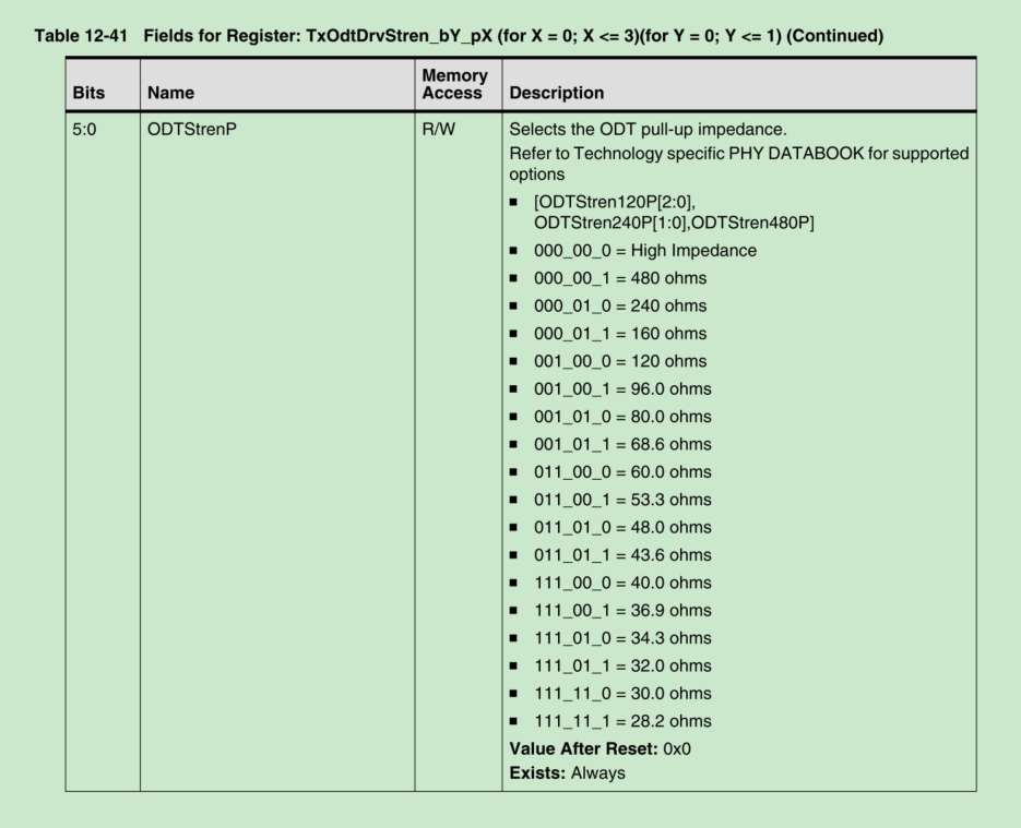
### PHY ODT
```c
//buildroot-overlay/boot/uboot/u-boot-2022.10-overlay/board/canaan/k230_canmv/k230pi_ddr_init_2133.c
//PHY ODT --pull up
//00_1000 0x08 Pullup/Down:120
//00_1010 0x0a Pullup/Down:80
//01_1000 0x18 Pullup/Down:60
//01_1010 0x1a Pullup/Down:48
//11_1000 0x38 Pullup/Down:40
//11_1010 0x3a Pullup/Down:34.3
reg_write( DDR_REG_BASE + 0x0001004d*4 +0x02000000 , 0x00000018 );
reg_write( DDR_REG_BASE + 0x0001014d*4 +0x02000000 , 0x00000018 );
reg_write( DDR_REG_BASE + 0x0001104d*4 +0x02000000 , 0x00000018 );
reg_write( DDR_REG_BASE + 0x0001114d*4 +0x02000000 , 0x00000018 );
reg_write( DDR_REG_BASE + 0x0001204d*4 +0x02000000 , 0x00000018 );
reg_write( DDR_REG_BASE + 0x0001214d*4 +0x02000000 , 0x00000018 );
reg_write( DDR_REG_BASE + 0x0001304d*4 +0x02000000 , 0x00000018 );
reg_write( DDR_REG_BASE + 0x0001314d*4 +0x02000000 , 0x00000018 );
```
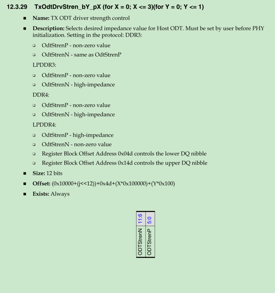
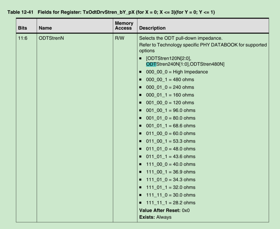
The complete meaning of the ODT register is as follows:
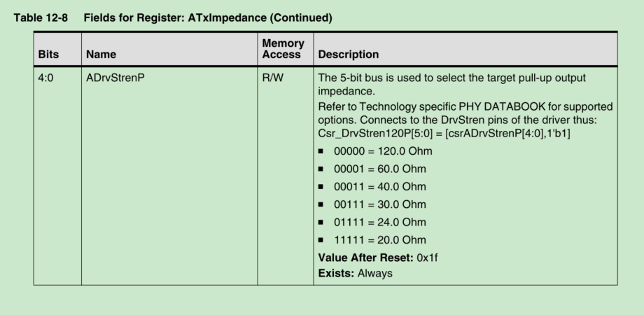
### PHY impedance
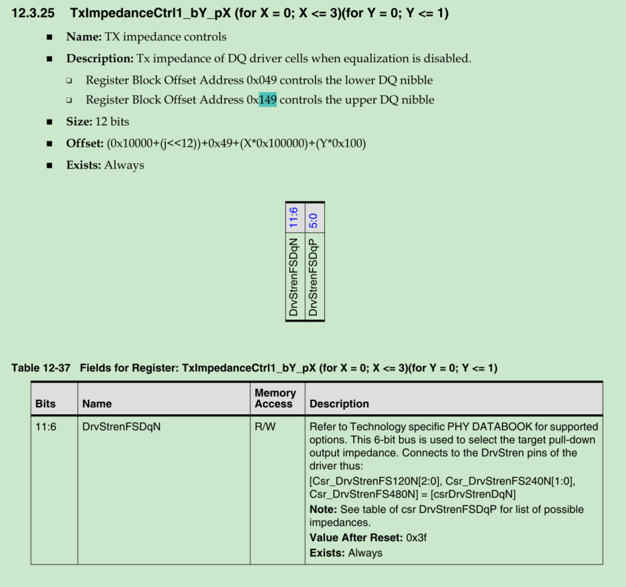
```c
////buildroot-overlay/boot/uboot/u-boot-2022.10-overlay/board/canaan/k230_canmv/k230pi_ddr_init_2133.c
//iteration place
//PHY TX output impedence
//0010_00 00_1000 0x208 Pullup/Down:120
//0010_10 00_1010 0x28a Pullup/Down:80
//0110_00 01_1000 0x618 Pullup/Down:60
//0110_10 01_1010 0x69a Pullup/Down:48
//1110_00 11_1000 0xe38 Pullup/Down:40
//1110_10 11_1010 0xeba Pullup/Down:34.3
reg_write( DDR_REG_BASE + 0x00010049*4 +0x02000000 , 0x00000E38 );
reg_write( DDR_REG_BASE + 0x00010149*4 +0x02000000 , 0x00000E38 );
reg_write( DDR_REG_BASE + 0x00011049*4 +0x02000000 , 0x00000E38 );
reg_write( DDR_REG_BASE + 0x00011149*4 +0x02000000 , 0x00000E38 );
reg_write( DDR_REG_BASE + 0x00012049*4 +0x02000000 , 0x00000E38 );
reg_write( DDR_REG_BASE + 0x00012149*4 +0x02000000 , 0x00000E38 );
reg_write( DDR_REG_BASE + 0x00013049*4 +0x02000000 , 0x00000E38 );
reg_write( DDR_REG_BASE + 0x00013149*4 +0x02000000 , 0x00000E38 );
//iteration place
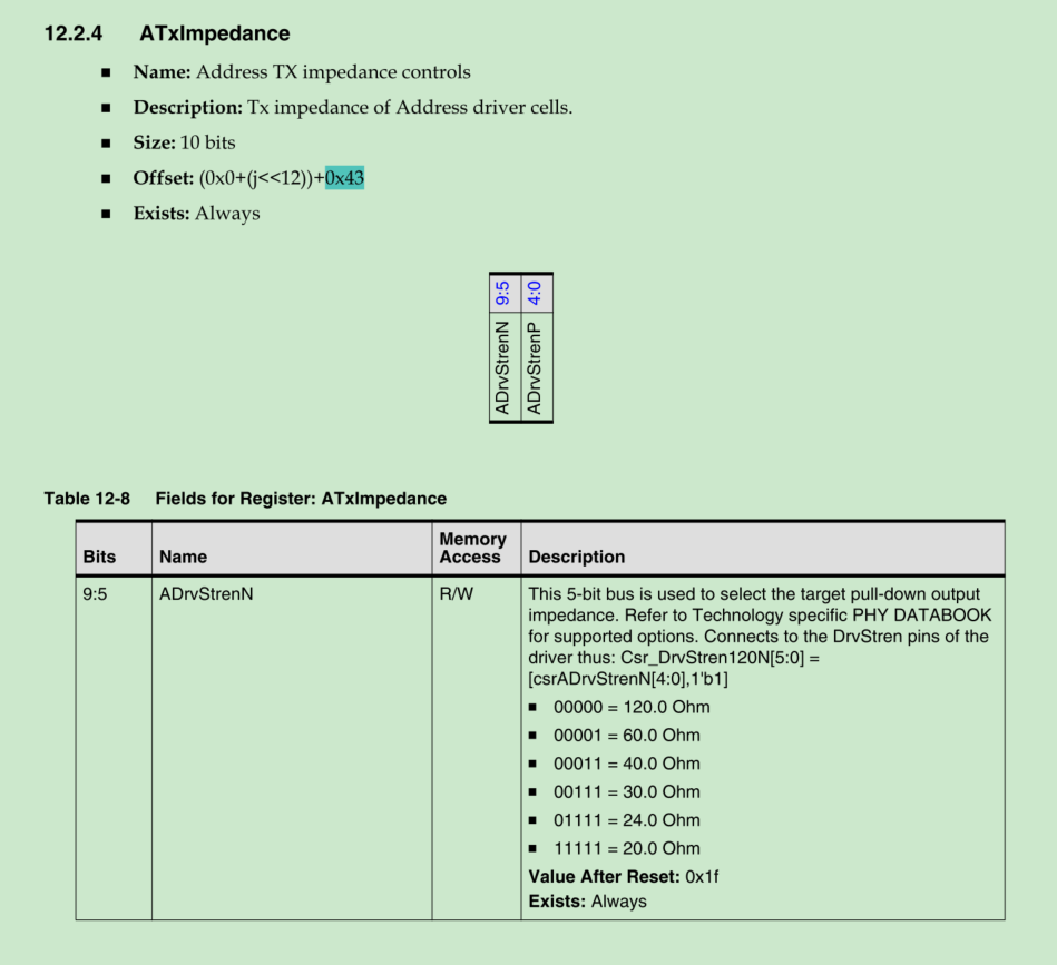
// PHY AC/CLK output impedence
//00000_00000 0x0 120
//00001_00001 0x21 60
//00011_00011 0x63 40
//00111_00111 0xe7 30
//01111_01111 0x1ef 24
//11111_11111 0x3ff 20
// // [phyinit_C_initPhyConfig] Programming ATxImpedance::ADrvStrenP to 0x1
// // [phyinit_C_initPhyConfig] Programming ATxImpedance::ADrvStrenN to 0x1
reg_write( DDR_REG_BASE + 0x43 *4+0x02000000,0x63);
reg_write( DDR_REG_BASE + 0x1043 *4+0x02000000,0x63);
reg_write( DDR_REG_BASE + 0x2043 *4+0x02000000,0x63);
reg_write( DDR_REG_BASE + 0x3043 *4+0x02000000,0x63);
reg_write( DDR_REG_BASE + 0x4043 *4+0x02000000,0x63);
reg_write( DDR_REG_BASE + 0x5043 *4+0x02000000,0x63);
reg_write( DDR_REG_BASE + 0x6043 *4+0x02000000,0x63);
reg_write( DDR_REG_BASE + 0x7043 *4+0x02000000,0x63);
reg_write( DDR_REG_BASE + 0x8043 *4+0x02000000,0x63);
reg_write( DDR_REG_BASE + 0x9043 *4+0x02000000,0x63);
```
The complete meaning of register 1 is as follows:
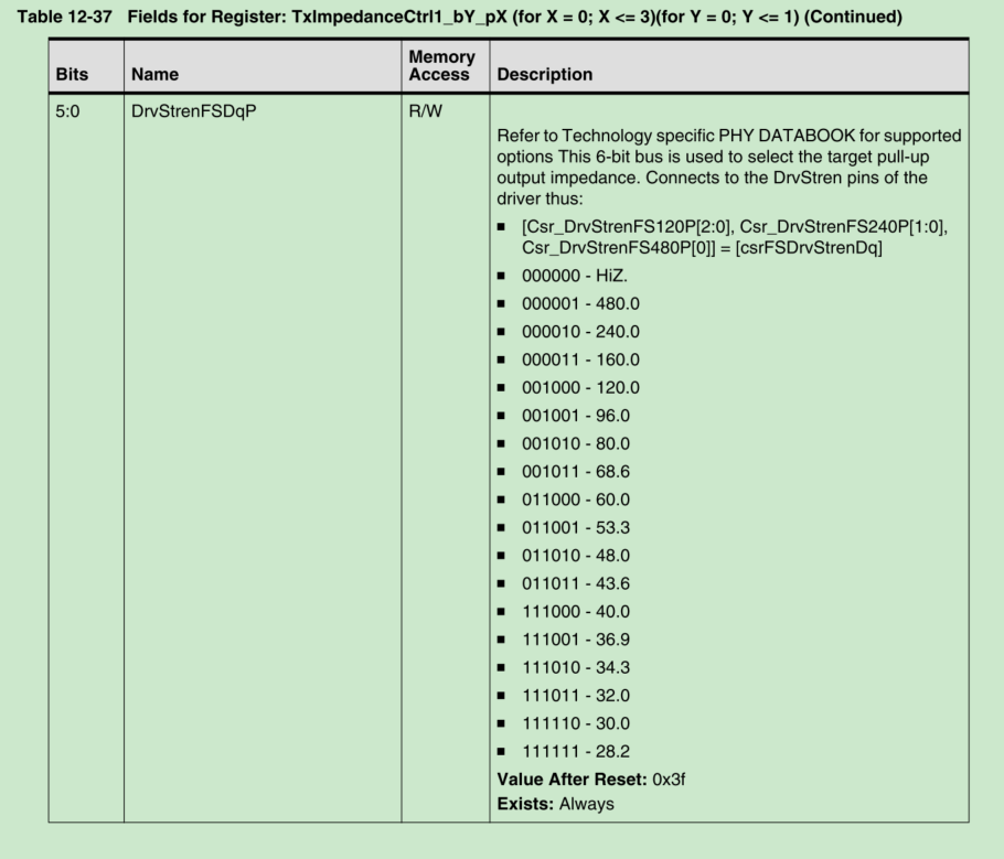
Register 2 definition:
### phy vref
```c
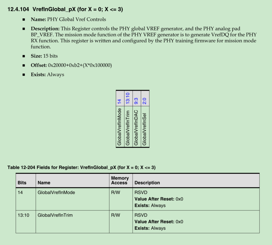
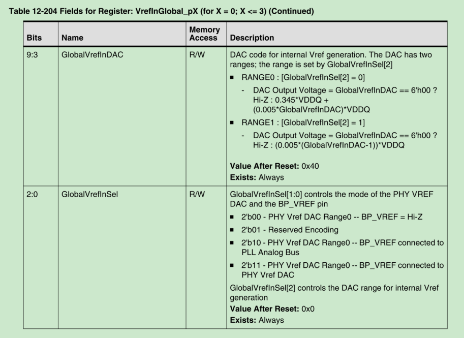
//iteration place
//PHY VERF
//INSEL VREFIN ALL Ratio
//---(0.005*X+0.345)VDDQ ---
//0x0 0x51 0x288 75% (GlobalVrefInSel to 0x0)
//0x0 0x41 0x208 67% (GlobalVrefInSel to 0x0)
//---(0.005*(X-1)VDDQ----
//0x4 0x65 0x32c 50% (GlobalVrefInSel to 0x4)
//0x4 0x33 0x19c 25% (GlobalVrefInSel to 0x4)
// // [phyinit_C_initPhyConfig] Pstate=0, Programming VrefInGlobal::GlobalVrefInDAC to 0x51
// // [phyinit_C_initPhyConfig] Pstate=0, Programming VrefInGlobal to 0x288
//reg_write( DDR_REG_BASE + 0x200b2*4+0x02000000,0x32c);//hyg
//reg_write( DDR_REG_BASE + 0x200b2*4+0x02000000,0x208);//hyg
//reg_write( DDR_REG_BASE + 0x200b2*4+0x02000000,0x32C);//hyg
reg_write( DDR_REG_BASE + 0x000200b2*4 +0x02000000 , 0x00000288 );
```
```c
//PHY VREF
// 0x40 50%
// 0x60 75%
// 0x56 67%
// 0x20 25%
reg_write( DDR_REG_BASE + 0x54006*4+0x02000000,0x60);
```
Register definition:
## DDR Stress Test
Execute the following commands to generate a DDR stress test image:
```bash
make
make ddr_test_img_128 ## Build a 128MB DDR stress test image (supports 128/512/1024/2048)
```
>Note 1: After startup, this image will continuously run the DDR stress test and will only stop when a memory error is detected. It is recommended to run it continuously for more than 24 hours to fully verify memory stability.
>Note 2: The test image is based on a bare-metal environment (without an operating system). After DDR initialization is complete, a dedicated stress test program is executed directly. This program repeatedly calls the VPU for encoding and decoding operations and verifies result consistency. Once a data abnormality is found, the test will be terminated.
## Attachments
### K230 DDR Related Pin Definition Table
| Function | Function Index | RTLBumpName | ball | DDR ballname_LP3_LP4 |
| -------------- | -------- | ----------- | ---- | --------------------- |
| | | BP_A[0] | N17 | DDR_CKE0_CKEA0 |
| | | BP_A[1] | P18 | DDR_CKE1_CKEA1 |
| | | BP_A[2] | T20 | DDR_CS0_CSA0 |
| | | BP_A[3] | T19 | DDR_CS1_CSA1 |
| | | BP_A[4] | R19 | DDR_CKP_CKAP |
| | | BP_A[5] | R20 | DDR_CKN_CKAN |
| | | BP_A[6] | | DDR_NC_NC |
| | | BP_A[7] | | DDR_NC_NC |
| CA/CAA | 0 | BP_A[8] | P19 | DDR_CA9_CAA5 |
| CA/CAA | 1 | BP_A[9] | M18 | DDR_CA8_CAA4 |
| CA/CAA | 2 | BP_A[10] | N20 | DDR_CA7_CAA3 |
| CA/CAA | 3 | BP_A[11] | N19 | DDR_CA6_CAA2 |
| CA/CAA | 4 | BP_A[12] | L16 | DDR_CA5_CAA1 |
| CA/CAA | 5 | BP_A[13] | M19 | DDR_CA4_CAA0 |
| CA/CAA | 6 | BP_A[14] | L17 | DDR_CA3_NC |
| CA/CAA | 7 | BP_A[15] | M20 | DDR_CA2_NA |
| CA/CAA | 8 | BP_A[16] | L20 | DDR_CA1_NC |
| CA/CAA | 9 | BP_A[17] | K20 | DDR_CA0_NC |
| CA/CAA | 10 | BP_A[18] | L18 | DDR_ODT_NC |
| | | BP_A[19] | | NC |
| | | BP_A[20] | | DDR_NC_CKEB0 |
| | | BP_A[21] | | DDR_NC_CKEB1 |
| | | BP_A[22] | | DDR_NC_CSB1 |
| | | BP_A[23] | | DDR_NC_CSB0 |
| | | BP_A[24] | | DDR_NC_CKBP |
| | | BP_A[25] | | DDR_NC_CKBN |
| | | BP_A[26] | | DDR_NC_NC |
| | | BP_A[27] | | DDR_NC_NC |
| CAB | 0 | BP_A[28] | E20 | DDR_NC_CAB0 |
| CAB | 1 | BP_A[29] | G19 | DDR_NC_CAB1 |
| CAB | 2 | BP_A[30] | G18 | DDR_NC_CAB2 |
| CAB | 3 | BP_A[31] | H17 | DDR_NC_CAB3 |
| CAB | 4 | BP_A[32] | F17 | DDR_NC_CAB4 |
| CAB | 5 | BP_A[33] | F19 | DDR_NC_CAB5 |
| | | BP_A[34] | | DDR_NC_NC |
| | | BP_A[35] | | DDR_NC_NC |
| | | BP_A[36] | | DDR_NC_NC |
| | | BP_A[37] | | DDR_NC_NC |
| | | BP_A[38] | | DDR_NC_NC |
| | | BP_A[39] | | NC |
| Byte 0/dbyte0 | 0 | BP_D[0] | U17 | DDR_DQ24_DQA7 |
| Byte 0/dbyte0 | 1 | BP_D[1] | Y18 | DDR_DQ25_DQA6 |
| Byte 0/dbyte0 | 2 | BP_D[2] | V18 | DDR_DQ26_DQA5 |
| Byte 0/dbyte0 | 3 | BP_D[3] | W18 | DDR_DQ27_DQA4 |
| Byte 0/dbyte0 | 4 | BP_D[4] | Y16 | DDR_DQ28_DQA3 |
| Byte 0/dbyte0 | 5 | BP_D[5] | V16 | DDR_DQ29_DQA2 |
| Byte 0/dbyte0 | 6 | BP_D[6] | T16 | DDR_DQ30_DQA1 |
| Byte 0/dbyte0 | 7 | BP_D[7] | U16 | DDR_DQ31_DQA0 |
| | | BP_D[8] | V17 | DDR_DM3_DMIA0 |
| | | BP_D[9] | W17 | DDR_DQS3P_DQSA0P |
| | | BP_D[10] | Y17 | DDR_DQS3N_DQSA0N |
| | | BP_D[11] | | NC |
| Byte 1/dbyte1 | 0 | BP_D[12] | R17 | DDR_DQ8_DQA8 |
| Byte 1/dbyte1 | 1 | BP_D[13] | T18 | DDR_DQ9_DQA9 |
| Byte 1/dbyte1 | 2 | BP_D[14] | R18 | DDR_DQ10_DQA10 |
| Byte 1/dbyte1 | 3 | BP_D[15] | U20 | DDR_DQ11_DQA11 |
| Byte 1/dbyte1 | 4 | BP_D[16] | W19 | DDR_DQ12_DQA12 |
| Byte 1/dbyte1 | 5 | BP_D[17] | U18 | DDR_DQ13_DQA13 |
| Byte 1/dbyte1 | 6 | BP_D[18] | P16 | DDR_DQ14_DQA14 |
| Byte 1/dbyte1 | 7 | BP_D[19] | T17 | DDR_DQ15_DQA15 |
| | | BP_D[20] | P17 | DDR_DM1_DMIA1 |
| | | BP_D[21] | V20 | DDR_DQS1P_DQSA1P |
| | | BP_D[22] | V19 | DDR_DQS1N_DQSA1N |
| | | BP_D[23] | | NC |
| Byte 2/dbyte2 | 0 | BP_D[24] | C17 | DDR_DQ0_DQB15 |
| Byte 2/dbyte2 | 1 | BP_D[25] | D16 | DDR_DQ1_DQB14 |
| Byte 2/dbyte2 | 2 | BP_D[26] | D17 | DDR_DQ2_DQB13 |
| Byte 2/dbyte2 | 3 | BP_D[27] | C18 | DDR_DQ3_DQB12 |
| Byte 2/dbyte2 | 4 | BP_D[28] | E18 | DDR_DQ4_DQB11 |
| Byte 2/dbyte2 | 5 | BP_D[29] | E17 | DDR_DQ5_DQB10 |
| Byte 2/dbyte2 | 6 | BP_D[30] | B19 | DDR_DQ6_DQB9 |
| Byte 2/dbyte2 | 7 | BP_D[31] | C19 | DDR_DQ7_DQB8 |
| | | BP_D[32] | D18 | DDR_DM0_DMIB1 |
| | | BP_D[33] | B18 | DDR_DQS0P_DQSB1P |
| | | BP_D[34] | A18 | DDR_DQS0N_DQSB1N |
| | | BP_D[35] | | NC |
| Byte 3/dbyte3 | 0 | BP_D[36] | C14 | DDR_DQ16_DQB0 |
| Byte 3/dbyte3 | 1 | BP_D[37] | D14 | DDR_DQ17_DQB1 |
| Byte 3/dbyte3 | 2 | BP_D[38] | B14 | DDR_DQ18_DQB2 |
| Byte 3/dbyte3 | 3 | BP_D[39] | A14 | DDR_DQ19_DQB3 |
| Byte 3/dbyte3 | 4 | BP_D[40] | A17 | DDR_DQ20_DQB4 |
| Byte 3/dbyte3 | 5 | BP_D[41] | B16 | DDR_DQ21_DQB5 |
| Byte 3/dbyte3 | 6 | BP_D[42] | C16 | DDR_DQ22_DQB6 |
| Byte 3/dbyte3 | 7 | BP_D[43] | B17 | DDR_DQ23_DQB7 |
| | | BP_D[44] | C15 | DDR_DM2_DMIB0 |
| | | BP_D[45] | B15 | DDR_DQS2P_DQSB0P |
| | | BP_D[46] | A15 | DDR_DQS2N_DQSB0N |
| | | BP_D[47] | | N |